|
Revised 5/9/2006 |
|
The HP 9100’s PC-Board ROM
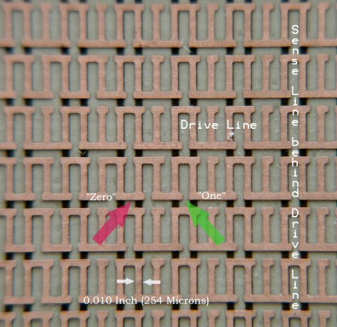
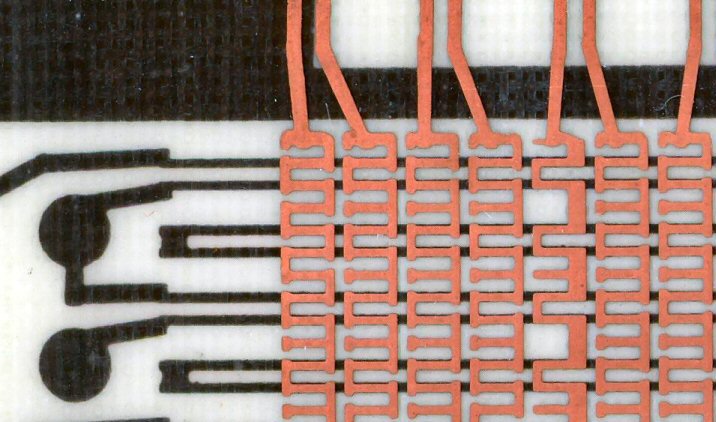
At each bit location, a sense loop in the pc-board ROM inductively coupled to two zig zags in the driven columns. If current flowed one direction through both legs of a bit-location zig zags, the current induced in the associated sense loop would produce a positive current spike in the sense loop. The result would be a logical one. However, if the two zig zags at a certain bit location were laid out so that the currents flowed in the opposite direction with respect to the two legs in the zig zags of a bit location, the currents would induce a negative current pulse the associated sense loop and would produce a logical zero. Near remembers the layout rule even today: “right for a zero and left for a one.” The differential nature of this design enhanced the memory’s reliability by vastly increasing noise immunity over a capacitively-coupled design. Near’s ROM design, refined by Osborne, eventually achieved a bit density of 1000 bits/in2. It employed a 16-layer printed-circuit board but very few active devices, which kept the cost of this very large memory device down. Unfortunately, multilayer pc-board technology of the day wasn’t able to produce a reliable high-capacity ROM. The problem was in the material used between the various layers of the multilayer board. A multilayer pc board is made by first producing a number of very thin double-sided boards. The HP 9100 ROM board consisted of a sandwich of eight double-sided boards. These double-sided boards are then sandwiched with a fiberglass mat impregnated with resin (the material is called “prepreg,” which means “pre impregnated”) and bonded together using heat to melt the resin and tremendous pressure. The HP 9100 ROM used seven prepreg layers between the eight double-sided circuit boards. However, the standard prepreg material’s electrical properties were sufficiently inconsistent to make the early prototype ROMs operate unreliably. There was too much electrical leakage through the prepreg, which caused the ROM board to operate incorrectly. Barney Oliver, the director of HP Labs, had been reading about a new space-age material called Teflon. It was supposed to have excellent electrical-insulation characteristics. At Barney Oliver’s suggestion, Near tried augmenting the prepreg layers with Teflon sheets. The Teflon did the job and became the “secret ingredient” in HP’s circuit-board ROM. Those Teflon sheets remained a secret ingredient and an HP trade secret for many years. Another of the pc-board ROM’s early problems was poor manufacturing yield. This problem fell on the shoulders of Tom Ligon, who had joined HP in 1966 after getting BS and MS degrees in physics from Oklahoma State University. Ligon had joined HP to work in HP Loveland’s new bipolar IC fab but his first assignment at HP was to tackle a strange seasonal variation in resistance that was affecting the precision, high-frequency wirewound resistors that HP’s Loveland Division made and sold as reference standards. The problem with the resistors turned out to be water absorption by the Mylar bobbin cores inside the resistors. When the Mylar absorbed water, it expanded and placed a strain on the resistor wire, thus changing its resistance noticeably. Ligon developed a special winding method for the resistors that relieved the stress, eliminated the need for a Mylar bobbin, and fixed the problem. Ligon then moved to the printed-circuit shop and tackled the yield problem with the HP 9100’s pc-board ROM. In Ligon’s words, the yields were “horrible.” He designed special production equipment and succeeded in raising the manufacturing yields of the complex, multilayer ROM but, he says, “The yields were never great.” All of this work was great preparation for Ligon’s next assignment: the development of HP’s first NMOS integrated-circuit fabrication process and a 4-Kbit IC ROM to completely replace the printed-circuit ROM technology.
|
|||||||||||||||||||||||||||||||||||||||||||
|
| [Home] [Prehistoric Times] [The 9100 Project] [Prologues] [The 9825 Projects] [Epilogues] |